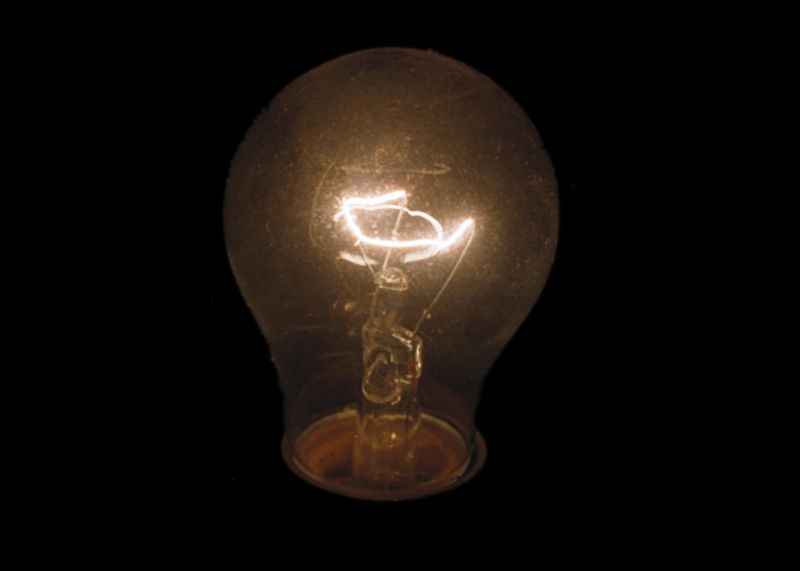
Enlarge / This probably isn’t the first lightbulb you’ve ever seen.
We spend a fair bit of energy creating stray electromagnetic fields in order to make sure our cellular and WiFi devices are constantly fed with data. Every now and again, someone suggests that there must be a way to harvest these fields in order to charge our devices wirelessly. Now, a team of researchers (a Swiss-Chinese-Swedish collaboration) has suggested a simpler option: use the light that we’re constantly flooding our rooms with instead.
The researchers have developed a new version of a technology—dye-sensitized solar cells—that so far hasn’t lived up to its promises. They found that, in the dim light typical of the indoors, their solar cells outperformed the extremely efficient versions we normally reserve for trips to space.
So sensitive
In most solar cells, electrons are generated in a semiconductor and pulled out by wires. Useful current is generated by a second set of wires that sends electrons back into the other side of the device. Efficiency is limited by the photovoltaic material itself, as well as the ability to pull electrons out of it before they simply hop back to where they originated.
Dye-sensitized solar cells work on very different principles. In some ways, “dye sensitized” is a misnomer. The dyes are actually the photovoltaic material, absorbing light and liberating electrons. Semiconductors are present, but all they do is grab the resulting electrons and pass them along as current. Electrons flow back into the system through an electrolyte, which carries electrons from external wiring and delivers them to the dye molecules, allowing the cycle to repeat.
These systems seem to have a number of advantages. For one, the dyes and semiconductor can be put in place through solutions processing, which is cheap and flexible compared to the production of silicon panels. And, by mixing in the right collection of dyes, it’s possible to tune the absorption of the devices to different wavelength ranges or broaden the wavelengths of light they absorb efficiently.
While all that seems promising, the field really hasn’t taken off. That’s in part because the dyes themselves are typically large, carbon-based molecules, which don’t conduct electrons as efficiently as many semiconductors. And, while they could probably be made cheaper, the astonishing drop in the price of silicon panels has made the price difference insignificant.
Continuing progress
But the new device indicates that the people who work in this field have not thrown in the towel (the authors include the person who helped pioneer modern dye-sensitized devices). It boasts a number of improvements large and small.
To begin with, the electrolyte used is copper-based, which eliminates the need for any rare and expensive metals. The copper is embedded in a cage of carbon-nitrogen rings, making it a bit bulkier. This is useful in combination with one of the dyes, which is also bulky. The combination of the two is enough to keep the copper from getting near the semiconductor that harvests charge, which would effectively short-circuit the panel.
Enlarge / The dyes can seamlessly integrate with packaging.
Freitag et. al.
Both dyes are pretty bulky and made of a long series of rings. These provide a conductive path to take the electrons from the tip of the dye (where the light-absorbing chemistry lives) to the base of the molecule, where the molecule attaches to the semiconductor. This distance decreases the likelihood that the electrons will flow from the semiconductor back out through the dye molecule to where they originated, which boosts the efficiency.
The base has also been engineered to interact with titanium dioxide, the semiconductor used here. And the conductive path through the dye matches the energy of the conducting band of the titanium dioxide.
The two dyes used here can be mixed together in different proportions, and the authors tested a variety of them to identify the most efficient combination. They ultimately settled on a combination that absorbs efficiently at all wavelengths from about 350 nanometers up to about 650 nanometers. Since the visible spectrum is generally defined as being between 400 and 700nm, this combination grabs most of it.
Performance
Out in the sunlight, the new device is nothing special. It produces a device efficiency of a bit over 11 percent. Given that silicon cells are well above 20-percent efficiencies, this isn’t likely to start a mass migration to the technology.
But internally, the device’s quantum efficiency seemed quite a bit better, as it was able to extract usable electrons from nearly every photon that was absorbed. The researchers write “the internal quantum efficiency ranges between 90 percent and practically 100 percent,” although there are some losses from the connections with the external wiring.
So they decided to give it a test under conditions where those photons were limited: indoor lighting. Even bright indoor lighting is typically only one percent of what you’d get on a sunny day. Unlike the Sun, most lights are also biased toward producing photons in the visible range—which nicely corresponds to the sensitivity of the device’s dyes.
Under indoor lighting, the device’s efficiency shot up to nearly 29 percent, close to the record for a single-material solar cell. So the researchers tested it against that record holder, gallium arsenide, which is expensive enough that it’s normally reserved for uses like space-based solar panels. And the dye-sensitized version won, with gallium arsenide’s efficiency dropping to about 20 percent in the dim light.
The authors estimate that just a couple of square centimeters would be enough to power a small sensor using nothing but ambient light. A panel of this material the size of a typical cellphone would produce about 30 milliWatts in a brightly lit room. That’s not enough to power the latest-and-greatest hardware, but it’s certainly enough to provide power to a variety of devices that can be useful to have around.
[“Source-arstechnica.”]