Table of Contents
ToggleCircuit Design Tips
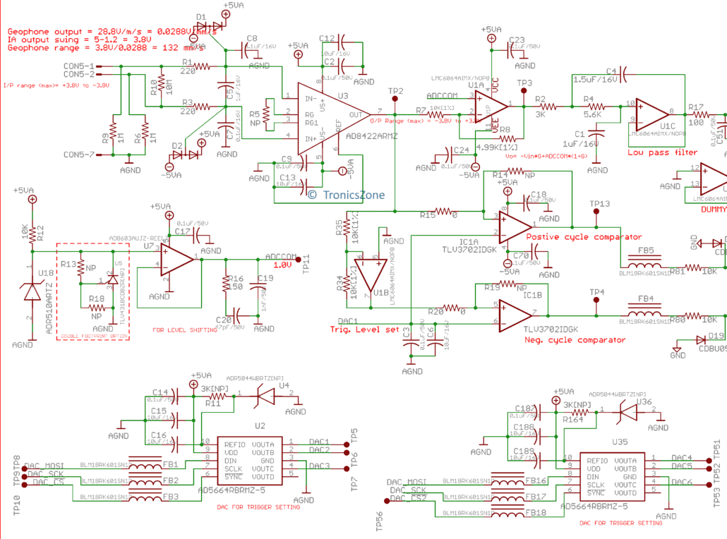
In electronic design, it is important to develop proper schematics of the circuit design for the success of the electronic product. An engineer must draw a neat and clean layout for the required circuit for the specific purpose by using the conventional method or going for Electronic Design Automation tools. Since drawing the schematic with the help of hands can lead to errors, so it is generally preferred to use certain EDA tools for better performance and efficiency of the circuits. Listed below are important tips to consider when designing the circuit layout.

Use of title block and block diagram
In electronics design, the block diagram is considered as the best guide that reflects the architecture and overview of the circuit schematic diagram. It aids the user to easily understand the function of the circuit and summarize the design systems.
Another vital aspect is to provide a title to the schematic diagram and append the name of the designer on the circuit’s title block as it provides a more proficient and professional look to the schematic. The schematic contains the essential notes and detail to construct the circuit layout on the PCB or breadboard.
Placements of I/O signals
The circuit layout in an electronic design should contain the flow of electrical signals drawn from left to right. To enhance the readability, the conventional practice of ground line at the bottom and the power line at the top of the circuit design layout is mostly followed.
The layout design is regarded as an artistic procedure as every designer needs to deliver proper care and attention in the component placement period by collecting the similar components together in the same and single direction, primarily the polarized components placed in a single column or row.
Most of the best ECAD provides easier pins and component placement options to enable the editing of the grids in the layout editor.
Make clear connections
In the circuit design, it is necessary to display and differentiate the nets to identify whether these nets are crossed over or connected. To resolve this problem, the designer should utilize the dot convention method to get a clear idea of the circuit connections. It is suggested to move at least a single grid point further before changing the direction when dealing with symbol pin connections. This measure makes sure that each net in the layout should be visible in its list when creating the layout of the PCB design.
To create a more concise schematic that elevates the readability of the user, use busses to cluster signals. Most of the good ECAD tools support this feature of grouping signals. To make various connections between disparate wires, a designer can add a global symbol or a connector to display general signals and invisible power pins like power and ground.
Utilize nets labels and brief reference designators
All the nets must be marked for the necessary signals in the circuit design schematic. This step mainly aids in the debugging process, or while running certain simulations. Though labeling of the nets is not necessary, however, it saves more time of the designer, especially in the PCB layout design. Moreover, labelling nets increases the readability for the users as it connects far terminals which are not even physically connected through a wire.
Another important aspect to keep in mind is the use of reference designators mentioned to display and acknowledge the component properly in the circuit design. These references help the designers to easily locate the components. The references must be mentioned nearby to the component in the schematic as per the type of pattern a designer chooses for the whole design.
Use of coupling/decoupling capacitors
In electronic devices, the supply of the power is unstable and delivers a fluctuating output voltage be fluctuating that can hamper the circuit. For this purpose, the designer uses different types of capacitor for filtering the input and output signals.
A decoupling capacitor is connected in parallel connection nearby the power source in the circuit design process to deliver pure DC supplies. These decoupling capacitors are used to decouple the incoming AC signals from DC signals. This capacitor initiates the charging process from the source point and when the voltage level of Vcc is achieved, the current ceased to flow through the capacitor as this decoupling capacitor maintains and keeps this flowing charge till any occurrence of the drop in the voltage level of Vcc from the source.
The coupling capacitors are majorly used when working with various amplifier circuits. These capacitors allow restricting and smooth flow of both the DC element and low-frequency noise in the output signals produced by the amplifier circuits. Hence, the coupling capacitors are majorly used for outcoming signals.
The use of bypass capacitor helps to remove intra and inter noise through the system by diverting the noise to the ground, especially in loudspeaker and amplifier circuits to achieve clear audio. Hence, these bypass capacitors are used to eliminate AC noise from the DC signals to receive a pure DC signal.
Make use of pull-down/pull up resistors
Every designer should consider the use of pull up and pull down resistors while working with digital IC and microcontroller circuits. This fundamental principle helps to ignore and tackle with the occurrence of the floating state.
All the digital ICs work with logic levels which are directly related to the input voltage. Let’s clarify this topic with the help of an example: Suppose the input voltage of a digital IC lies between +2.8 volts to 5 volts, so it will be considered as Logic 1 or high state and the voltage range of +0V to +0.8V will be considered Logic 0 or low state. On the other hand, the input voltage of +0.9V to +2.7V will be considered as floating state an indeterminate state and the logic state will be either consider a high (1) or a low(0). To bypass this scenario, the designer uses pull up and pull down resistors to enforce the suitable voltage required by the input pins of the IC chip, so that the circuit behaves accurately.
Microcontroller based circuit design
The use of microcontrollers will help the designer to save a lot of time and minimize the size of the layout by removing various components that are involved in analog-to-digital conversion. As a microcontroller chip contains various functions which can be programmed as per the requirements of the circuit design.
Nowadays, modern microcontrollers from various brands provide certain advanced features at reasonable prices to acquire different tasks like A/D conversion, Serial /SPI/ I2C communication timers, and many more other functions which are all accumulated in these small packages that increase the performance and the efficiency of the circuit design and acquire less space.
Use of PWM signals for less power consumption
It is important to design a circuit which consumes less energy for the final products that cannot replace the battery cells or cannot be charged. Due to this reason, the designer should always use the scheme of pulse width modulation (PWM) with the help of a reliable microcontroller or NE555 IC, which can enhance the energy capability of the application. Such a method can be utilized to consume less energy from the motor or LED circuits.
Selecting proper standards for designing component symbols
To initiate the schematic of the circuit design, it is important to consider the symbols of the components which are used in the layout drawing. Though these symbols are internationally employed, however, there may be a different representation of these symbols in other parts of the world. To resolve this issue, the Institute of Electrical and Electronics Engineers (IEEE) has created several standards which can be used by the designers for mostly used components like IEEE Standard 991 which is used for logical circuit diagrams, IEEE Standard 315 that contains designation and graphic symbols for various diagrams in the field of electrical and electronics and IEEE Standard 91which contain several graphic symbols of various logic functions.
Selection of proper CAD tool
Circuit design can be easily drawn with the help of hands for simple schematic designs even if the designer is not a pro. However, when it comes to constructing complex circuit designs, it is necessary to use appropriate electronic computer-aided design (ECAD) software. This ECAD software is commonly mentioned by the client in his/her job description or chosen by the company itself. Otherwise, it is mostly suggested to make use of a professional CAD tool from renowned developers which can create schematic as well as the layout designs of the PCB in 3D views, artwork, bill of materials and Gerber files when going for final production of the product.
Several EDA firms and developers provide free ECAD tools like KiCAD, while some provide paid ECAD tools such as Altium Designer, OrCAD etc. It depends on the designer which software is suitable for the circuit design process.
At last, it is best to master the ECAD tool that works well for the designer. Though it is good to know about manipulating EDA software, however, it is better to learn the designing technique of drawing and building the circuit.
[“source=tronicszone”]
| M | T | W | T | F | S | S |
|---|---|---|---|---|---|---|
| 1 | 2 | 3 | 4 | 5 | 6 | 7 |
| 8 | 9 | 10 | 11 | 12 | 13 | 14 |
| 15 | 16 | 17 | 18 | 19 | 20 | 21 |
| 22 | 23 | 24 | 25 | 26 | 27 | 28 |
| 29 | 30 | |||||


